
Expert Engineering for Advanced PCB Layouts
Leverage over 30 years of specialized PCB design engineering expertise. From complex schematics to manufacturable ready boards with optimized signal integrity, robust power distribution and DFM/DFT designed in from the start.
PRINCIPAL PCB DESIGN ENGINEER CONSULTANT
- 30+ years of PCB layout & engineering consulting.
- High-impact layout for companies demanding uncompromising hardware reliability.
- From complex schematics into manufacturing ready boards, optimizing signal integrity, robust power distribution and seamless DFM/DFT integration.
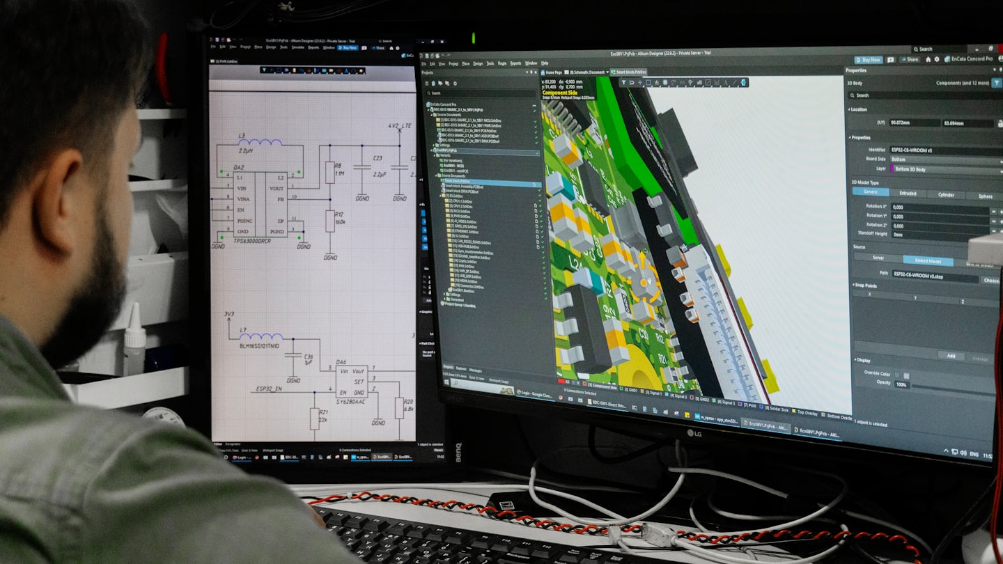
- Fluent in Altium Designer and Siemens PADS Professional.
CORE TECHNICAL CAPABILITIES
From schematic to fabrication-ready artwork
Every board is engineered for signal performance, power integrity, and clean manufacturing handoff — not just routed to fit.

01 – Advanced Layout & Routing
Multi-layer HDI and rigid-flex design
High-speed digital, analog & mixed-signal placement
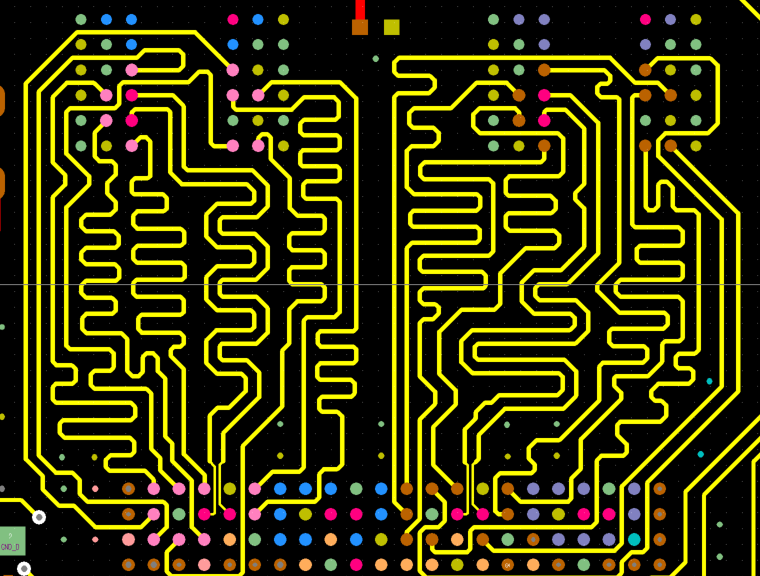
Differential pair routing, length matching & serpentine delay compensation

02 – Stack-Up & Impedance Control
Custom layer stack-ups for signal performance & EMI reduction
Dielectric selection & controlled-impedance calculation (40-100 ohm)
Return path continuity & reference plane optimization

03 – Signal & Power Integrity
High-speed bus optimization: DDR, PCIe, Ethernet, USB
PDN design, decoupling placement & loop-inductance minimization
Crosstalk, reflection & ground-bounce mitigation
04 – DFM / DFT & Fabrication Packages
Rigorous DFM & DFA verification
Complete Gerber, OOB++, IPC netlist & assembly packages
Direct collaboration with fabricators for high first-pass yield
THE CLIENT ADVANTAGE
Deep layout bandwidth, exactly when you need it
Streamlined consulting workflow ensures precision PCB design from initial schematic review to final manufacturing files.
1 – Eliminate Costly Respins
Layout, trace geometry, and stack-up get it right on the first iteration.
2 – Accelerated Schedules
Focused layout bandwidth exactly when your team needs to hit critical milestones.
3 – Flawless Handoffs
Deliverables verified against strict industry standards to prevent manufacturing bottlenecks.
4 – Seamless Tool Integration
Proficient in Altium Designer and Siemens Graphics PADS — plug directly into your internal engineering workflows.
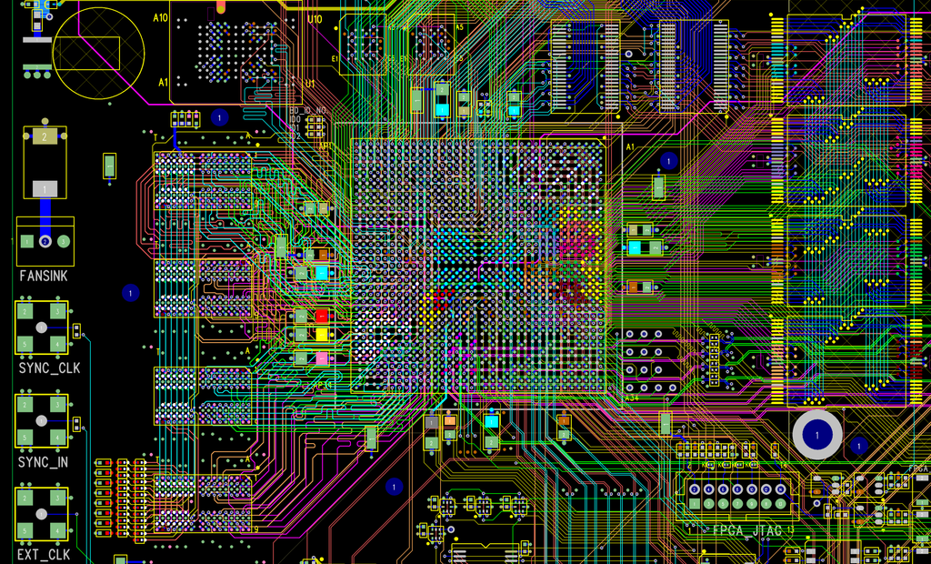
Advanced Layout
High-density routing and placement tailored to meet strict industry standards.
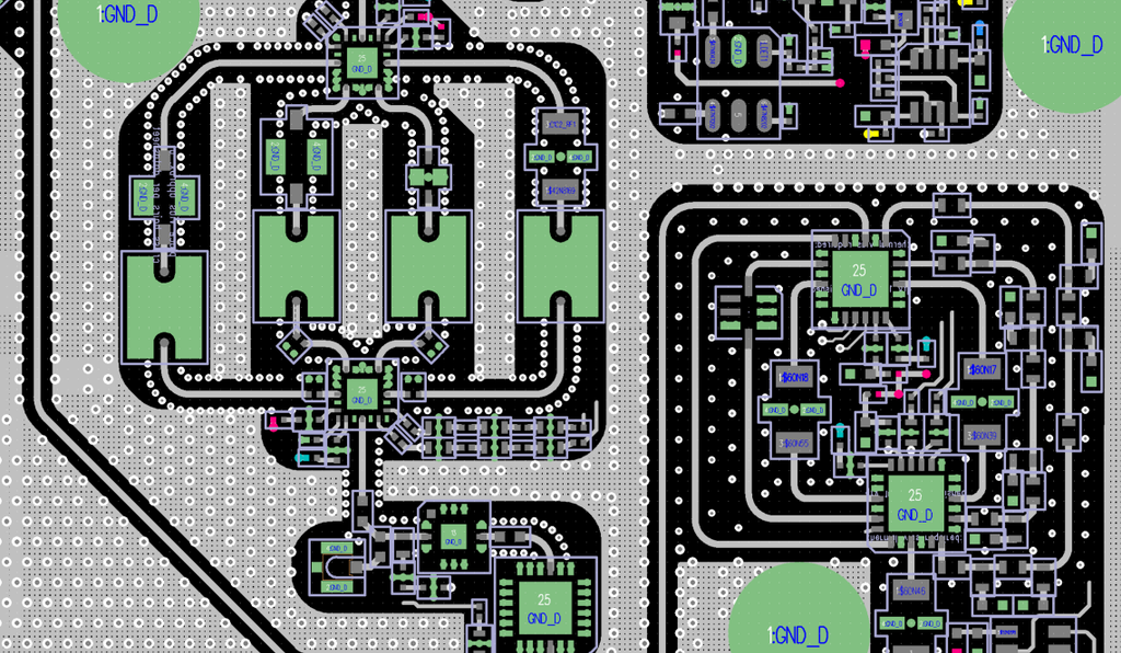
Impedance Control
Precise stack-up design for optimal signal and power integrity performance.
DFM/DFT Practices
Ensuring flawless manufacturing and testing readiness for seamless production.